
Si nanowires (NWs) attract significant attention because of their potential applications such as vertically integrated NW field effect transistors, bio-chemical sensors, photovoltaic, thermoelectric devices, lithium battery anodes and so on. Si NWs can be fabricated using chemical vapor deposition, laser ablation, thermal evaporation, and solution methods. For certain applications, Si NWs are preferred to form on the substrate different from Si. For example, cost and flexibility may be concerned for solar cells, so metal films, glass, or plastics are preferred. Biocompatibility, light weight, and transparency are important factors for bio-chemical sensing, so glass or plastics are better than Si. The formation of Si NWs on alien substrates has been achieved using methods such as chemical vapor deposition. Si NWs have been grown on stainless steel film, but the growth and process temperature is above 650 oC, which is not suitable for plastics or glass substrate. Transfer of Si NWs from Si substrate to alien substrates has been proposed and demonstrated for thermoelectric and photovoltaic applications. Even hundreds of pre-aligned silicon NWs onto plastic has also been achieved. However, those transferred Si NWs are horizontally aligned, limiting the NW density. In addition, they use the expensive Si-on-insulator (SOI) wafer to start with. Thus the cost is actually large although the devices are fabricated on the cheap plastic. Here we demonstrate the massive transfer of over millions of Si NWs fabricated from the usual Si wafer onto glass with the density of about 3 - 5 x 10⁷ Si NWs/mm2. The transferred Si NWs have nearly identical orientation and are vertically aligned on the glass substrate. The X-ray diffraction investigation reveals that the transferred NWs exhibit almost the same crystal property as the bulk Si. Their characteristics are investigated. The absorption characteristics of the transferred Si NWs are ignificantly modified over the spectral range of 400 - 1100 nm. More than 30-fold enhancement of absorption coefficient was found in the near infrared (IR) range.
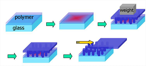
(a) The receiver substrate spin-coated with polymer thin film is heated.
(b) The Si NWs are pressed against the glass substrate.
(c) The whole setup is cooled down until the temperature dropped below the glass transition temperature of polymer.
(d) To remove the original Si substrate.
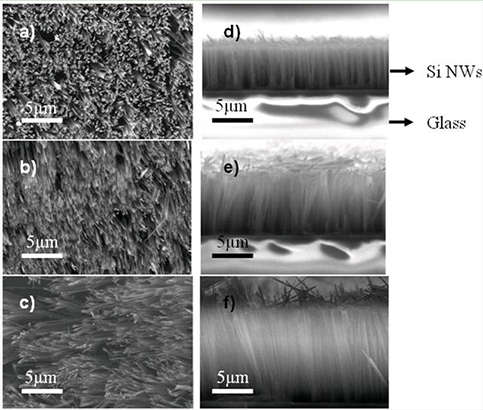
(a)-(c) The top-view SEM images of transferred Si NWs.
(d)-(f) The side-view SEM image of transferred Si NWs on glass substrates.
The lengths of transferred Si NWs are 5.07μm, 6.98μm, and 10.84 μm, respectively.
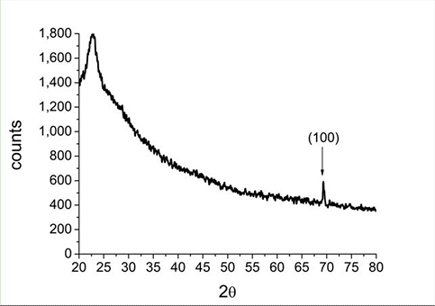
suggesting that transferred Si NWs exhibit total (100) preferential orientation. A broad featureless peak,centered at about 22°, is assigned to the amorphous silica of the receiver substrate.
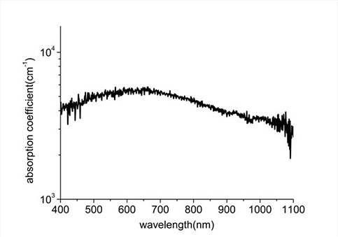
The absorption coefficient is about 3×103 cm-1 at the wavelength of 1100 nm and increases to a maximum of 5.5×103 cm-1 at 650 nm.