
Polymer solar cells (PSCs) have attracted much attention due to their great potentials for large-area, light-weight, flexible, and low-cost devices. Recently, bulk-heterojunction (BHJ) solar cells based on poly(3-hexylthiophene) (P3HT) and (6,6)-phenyl C61 butyric acid methyl ester (PCBM) with power conversionefficiency (PCE) of 4-5 % have been reported. However, control of the transportation of the charge carriers at interfaces is one of the most challenging issues in the improvement of PSCs. It has been reported that the insertion of an interlayer between the organic layer and the anode improves the device performance. To date, poly(3,4-ethylenedioxythiophene):poly(styrenesulfonate) (PEDOT:PSS) and transition metal oxides have been employed for this purpose. However, only the deposition of PEDOT:PSS layer can be easily processed by solution-based coating techniques. Most transition metal oxides as the anode interlayers are deposited by the vacuum evaporation, which could detract from the advantage of the ease of PSC fabrication. Using solution-processed transition metal oxide as the anode interlayer for improving the PSC performance has seldom been reported.
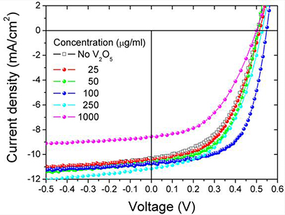
The aim of this work is to realize a low-cost and high-efficiency inverted PSC hybridized with ZnO nanorod arrays by introduction of a solution-processedvanadium oxide (V2O5) as the anode interlayer. Our investigation shows that the photovoltaic device performance is improved by the introduction of the V2O5interlayer due to the efficient suppression of the leakage currents at the organic/metal interface. Compared to the conventional BHJ structure (indium tin oxide(ITO)/PEDOT:PSS/active layer/Al), the use of the inverted structure overcomes some obstacles such as the facile oxidation of Al and the electrical inhomogeneities of PEDOT:PSS as well as its corrosion to ITO. The inverted PSCs utilize an air-stable high work-function electrode as the back contact to collect holes and metal-oxide nanostructures at the ITO to collect electrons. Furthermore, it has been reported that the ZnO nanorods have beneficial effects of collecting and transporting electrons in the inverted PSCs hybridized with the ZnO nanorods. Our works combine these advantages of V2O5 interlayer and ZnO nanorods, which thereby suppress the leakage currents and improve the collection and transportation of the charge carriers, resulting in enhancements of PCE, open-circuit voltage (VOC), and fill factor (FF) of the devices. In addition, the V2O5 interlayer can serve as an optical spacer to increase light absorption, leading to an increased short-circuit density (JSC). Moreover, the V2O5 interlayer and ZnO nanorod arrays both are fabricated from simple solution-based processes, which are well-suited for use in high-throughput roll-to-roll manufacturing.Although PEDOT:PSS layer can be solution processed, its hygroscopic nature is likely to form insulating patches due to the water adsorption, thus degrading the devices. In contrast, V2O5 is relatively insensitive to water and stable in air. The solution-processed V2O5 interlayer can serve as a barrier preventing oxygen or water from entering and degrading the photoactive layer. In addition, this approach does not need annealing treatment like PEDOT:PSS nor vacuum equipments, so it is simple, expeditious, and effective. This is very important for commercial realization of low-cost and large-area printed solar cells.
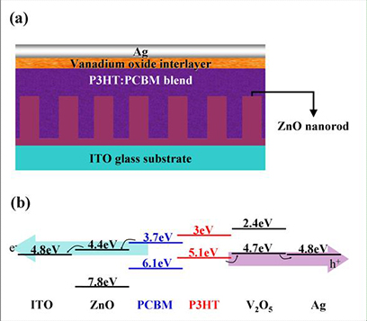
- Device structure of the photovoltaic cells.
- Energy band diagram for the photovoltaic cells in this study
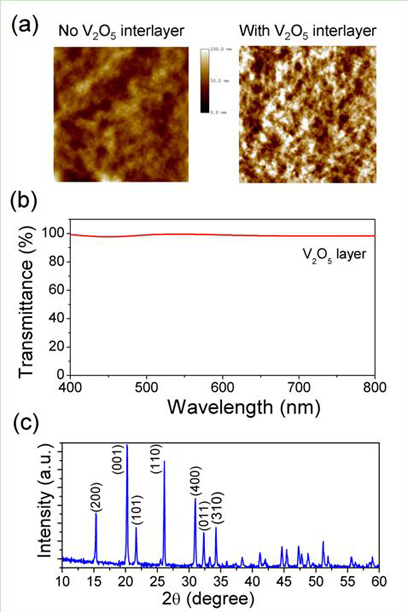
- AFM images of the photoactive layers covered with and without the optimum V2O5 interlayer. AFM image scans are 5×5 μm.
- Transmissionspectrum of the V2O5 layer (from the 100 μg/ml V2O5 colloidal solution) on a glass substrate.
- XRD spectrum of V2O5.
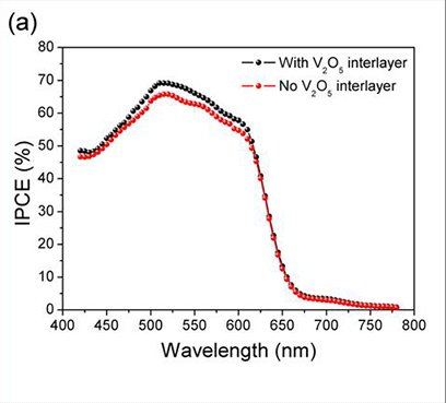
- IPCE spectra for the devices with and without the optimum V2O5 interlayer.
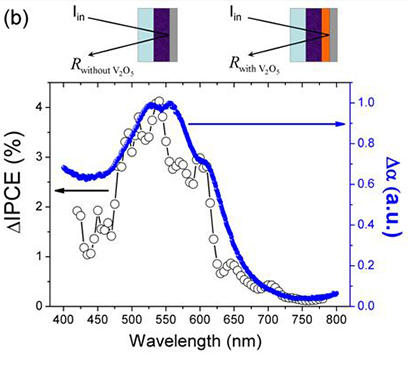
- The change in absorption spectrum [Δα(λ)] and the difference in IPCE spectrum [ΔIPCE(λ)] resulting from the insertion of the optimum V2O5 interlayer. The inset is a schematic of the optical beam path in the both samples. The variables are defined in the text.