Because of the significant increase of petroleum and greenhouse effect caused by the carbon dioxide generated from the burning carbon-related fuel, there is an urgent need of using alternative energy, in particular, the renewable energy sources. Among those renewable energy sources, using solar energy is the most attractive for its abundant supply form the sun and clean, no pollution characteristics. However, current solar cells are mainly made from bulk Si or bulk III-V semiconductors. Unfortunately, those types of solar cells need large amount of raw materials, causing the high cost of production. Thus thin-film solar cells are regarded as good solutions to reduce the material usage.
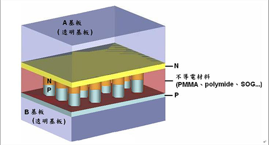
We propose a novel technique to develop crystalline semiconductor thin-film solar cells. As shown in Fig. 1, the concept is to transfer crystalline Si nano/micro- structure or III-V compound nano/micro-structure onto alien substrates to fabricate solar cells without lattice-matched concern. This thin-film solar cell with high crystal quality presents high power conversion efficiency. Besides, the thin-film type offers the advantages of large-area fabrication and the bending flexibility.
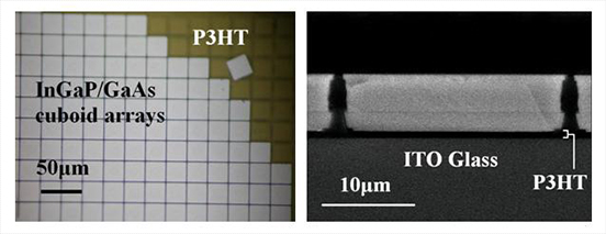
The following is the transfer technique we have developed. InGaP/GaAs double-junction square-based (25μm×25μm) micro-cuboid arrays were released from GaAs substrate by the epitaxial lift-off process. These InGaP/GaAs micro-cuboid arrays were transplanted to the P3HT film spun on ITO glass substrate successfully. Besides the significant cost reduction, our method shows the rapid transplantation and the potential for high-efficiency large-area devices fabrication.
As a result of the ability to tune the band-gap of III-V compound semiconductor materials to match the solar spectrum, solar cells made from these materials have unsurpassed conversion efficiencies. The most frequently used materials for III–V solar cells such as GaAs and InGaP are direct band gap semiconductors with high absorption coefficients. A stack with a thickness of only a few micrometers of these materials is required to absorb all light that the cell can convert into electricity. However, III–V solar cells are usually not referred to as thin-film cells. The reason why III–V cells are not referred to as thin- film, is that the cell structures are generally deposited on an approximately hundred-μm-thick GaAs or Ge wafer in order to obtain single crystal solar cell structures.
However, after the deposition of the solar cell film, the substrate is of no further use for its performance. The reduction of the costs of III–V semiconductor materials and an increase of the power to weight ratio is highly desired. The most successful method to achieve these goals is epitaxial lift-off (ELO). This method uses a very thin (5-50nm) sacrificial AlxGa1-xAs (x>0.6) release layer which is grown between the device and the GaAs substrate. The thin film device is released from its host substrate by selective etching of the AlxGa1-xAs release layer with aqueous HF solution, together with the compressive strain induced by a wax layer. Owing to the large selectivity (>106) of the HF solution for etching of AlGaAs over GaAs, the original substrate is not affected and can be reused.
A high lateral etch rate is considered essential for industrial applications for ELO technique. Therefore, recently lateral etch rate as obtained by different approaches of the ELO method has been elaborated in literature, including preparing the samples with wax and submerging them in the HF solution until the thin films were found floating in the solution after several hours or up to several days, the weight-induced ELO process (WI-ELO), and ELO with a stabilized radius of curvature by guiding the temporary flexible carrier over a cylinder surface. A disadvantage of the weight-induced ELO process is that the flexible carrier easily bends too much. This will results in cracking of the epitaxial layer structure. For this reason, the ELO process with a stabilized radius of curvature by guiding the temporary flexible carrier over a cylinder surface was developed. For the above-mentioned approaches, the larger area of the lifted off epi-film, the longer time of the ELO etching process and the greater risk of microscopic cleavage cracks. In order to shorten the ELO etching time and prevent the microscopic cleavage cracks, we develop a unique transplantation method.
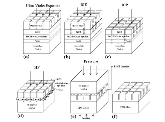
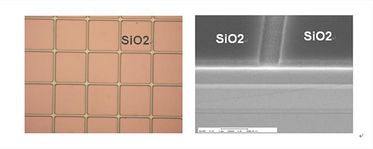
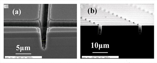
substrate, thin sacrificial AlAs release layer were grown. After the epi-film growth, thick silicon dioxide (SiO2) layer was grown by PECVD. Afterward photo resist was spun on SiO2 layer and proceed with UV photolithography as shown in Fig. 2(a). The size of each small cubic in the periodic patterns is 25μm×25μm. After photolithography, the patterns were transferred into the SiO2 layer coated on double-junction device by reactive ion etching (RIE) as shown in Fig. 2(b) and then the photoresist was removed. The etching time was optimized to ensure a reliable pattern transfer, and at the same time to cause the minimum damage to the surface of double-junction device. After the RIE etching, the periodic square-based (25μm×25μm) patterns were precisely transferred to the SiO2 mask template as shown in Fig. 3, with a slight increase of the linewidth less than 5%.
(a) Slots etched by ICP process,
(b) Square-based micro-cuboid arrays
substrate, thin sacrificial AlAs release layer were grown. After the epi-film growth, thick silicon dioxide (SiO2) layer was grown by PECVD. Afterward photo resist was spun on SiO2 layer and proceed with UV photolithography as shown in Fig. 2(a). The size of each small cubic in the periodic patterns is 25μm×25μm. After photolithography, the patterns were transferred into the SiO2 layer coated on double-junction device by reactive ion etching (RIE) as shown in Fig. 2(b) and then the photoresist was removed. The etching time was optimized to ensure a reliable pattern transfer, and at the same time to cause the minimum damage to the surface of double-junction device. After the RIE etching, the periodic square-based (25μm×25μm) patterns were precisely transferred to the SiO2 mask template as shown in Fig. 3, with a slight increase of the linewidth less than 5%.
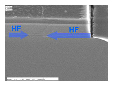
Then the sample was submerged in the aqueous HF solution to etch the sacrificial AlAs layer and the remaining SiO2 mask template after ICP etching as shown in Fig. 2(d). The ELO submerged time must be shorter than the etch time required to completely release the epi-film from the GaAs substrate. After the rapid wet etching of AlAs layer, there were very tiny AlAs which can remain beneath each cuboid. This tiny AlAs not only fixed each cuboid on GaAs substrate but also can be snapped easily, as shown in Fig. 5.
(Left: top-view, right: cross-section)
We have successfully transferred InGaP/GaAs double-junction square-based (25μm×25μm) micro-cuboid photovoltaic arrays onto the P3HT film spun on ITO glass substrate using the epitaxial lift-off (ELO) technique. Comparing with the conventional ELO method, including WI-ELO and ELO with a stabilized radius of curvature, our new method shortens the lifted-off time greatly. Besides, for the above-mentioned approaches, when the area of the lifted off epi-film becomes larger or the application of the device becomes more bending, the microscopic cleavage cracks may occur. This will limit its application and performance. However, our new method shows the rapid transplantation and the potential for large-area devices fabrication simultaneously without the cracking concern. It is expected that a large variety of substrates and much larger area of III-V thin film photovoltaic devices can be used for versatile applications in the future.