國立台灣大學林清富教授實驗室
研究領域摘要
主題三: 矽奈米線太陽能電池應用
研究人員: 許書嘉
英文摘要:
Si nanowires (NWs) attract significant attention because of their potential applications such as vertically integrated NW field effect transistors, bio-chemical
sensors, photovoltaic, thermoelectric devices, lithium battery anodes and so on. Si NWs can be fabricated using chemical vapor deposition, laser ablation,
thermal evaporation, and solution methods. For certain applications, Si NWs are preferred to form on the substrate different from Si. For example, cost and
flexibility may be concerned for solar cells, so metal films, glass, or plastics are preferred. Biocompatibility, light weight, and transparency are important factors
for bio-chemical sensing, so glass or plastics are better than Si. The formation of Si NWs on alien substrates has been achieved using methods such as chemical
vapor deposition. Si NWs have been grown on stainless steel film, but the growth and process temperature is above 650 oC, which is not suitable for plastics or
glass substrate.
Transfer of Si NWs from Si substrate to alien substrates has been proposed and demonstrated for thermoelectric and photovoltaic applications. Even hundreds of
pre-aligned silicon NWs onto plastic has also been achieved. However, those transferred Si NWs are horizontally aligned, limiting the NW density. In addition,
they use the expensive Si-on-insulator (SOI) wafer to start with. Thus the cost is actually large although the devices are fabricated on the cheap plastic. Here we
demonstrate the massive transfer of over millions of Si NWs fabricated from the usual Si wafer onto glass with the density of about 3 - 5 x 10⁷ Si NWs/mm2.
The transferred Si NWs have nearly identical orientation and are vertically aligned on the glass substrate. The X-ray diffraction investigation reveals that the
transferred NWs exhibit almost the same crystal property as the bulk Si. Their characteristics are investigated. The absorption characteristics of the transferred Si
NWs are significantly modified over the spectral range of 400 - 1100 nm. More than 30-fold enhancement of absorption coefficient was found in the near
infrared (IR) range.
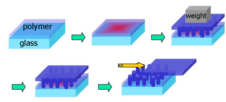
Figure 1 Illustration of massively transferring vertically-aligned Si NWs.
(a) The receiver substrate spin-coated with polymer thin film is heated.
(b) The Si NWs are pressed against the glass substrate.
(c) The whole setup is cooled down until the temperature dropped below the glass transition temperature of polymer.
(d) To remove the original Si substrate.
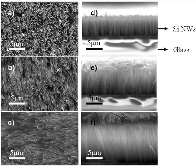
Figure 2 SEM images of transferred Si NWs on glass substrates at the impressing pressure about 55 kg/cm2.
(a)-(c) The top-view SEM images of transferred Si NWs.
(d)-(f) The side-view SEM image of transferred Si NWs on glass substrates.
The lengths of transferred Si NWs are 5.07μm, 6.98μm, and 10.84 μm, respectively.
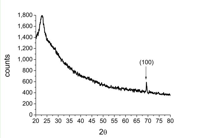
Figure 3 X-ray diffraction spectrum. A sharp peak corresponding to silicon (100) is observed at 69°,
suggesting that transferred Si NWs exhibit total (100) preferential orientation. A broad featureless peak,
centered at about 22°, is assigned to the amorphous silica of the receiver substrate.
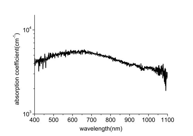
Figure 4 The estimated absorption coefficient of transferred Si NWs.
The absorption coefficient is about 3×103 cm-1 at the wavelength of 1100 nm and increases to a maximum of 5.5×103 cm-1 at 650 nm.
中文摘要:
矽奈米線吸引很多的注意,這是由於他很有潛力應用於場效電晶體、生化感測器、熱電元件等等。矽奈米線的製作可以使用化學氣相沈積法、
雷射法、熱蒸鍍法、和溶液法。在一些應用當中,矽奈米線需要製作於其他基板上,例如在可撓基板上的應用,玻璃或塑膠基板,然而以目前
的方法要將矽奈米線製作於其他基板上,遇到很大的障礙,因為目前的製程環境需要高溫650度以上,玻璃和塑膠基板都無法承受這樣的高溫環
境。
轉移矽奈米線於異質基板上已經有應用於熱電元件與太陽能元件的應用,數百根的奈米線可以被轉移,然而這些奈米線是平行於基板方向,而
限制奈米線的密度,且這些奈米線必須先製作於昂貴的SOI基板上才易於轉移,這使得成本大大地提昇。這裡我們展示可以大量轉移直立矽奈米
線於異質基板上,奈米線的密度達到3 - 5 x 10⁷ Si NWs/mm2。轉移的矽奈米線具有相同的晶格方向性,且於直立排列於基板上。我們研究轉移奈
米線的光學特性,發現轉移於玻璃基板上的矽奈米線的吸收係數產生很大的變化,在紅外光區域的吸收係數增加超過30倍,這項研究成果的發
現,將使矽奈米線在未來很有潛力應用於太陽能電池,增加紅外光區域的吸收。